- 您现在的位置:买卖IC网 > Sheet目录2003 > LTC1411IG#TRPBF (Linear Technology)IC A/D CONV 14BIT 2.5MSPS 36SSOP
7
LTC1411
1411f
DVP (Pin 30): 5V Digital Power Supply Pin. Bypass to
OGND with a 10
F tantalum capacitor.
DGND (Pin 31): Digital Ground.
CONVST (Pin 32): Conversion Start Signal. This active
low signal starts a conversion on its falling edge.
PGA1, PGA0 (Pins 33, 34): Logic Inputs for Program-
mable Input Range. This ADC has four input ranges (or
four REFCOM2 voltages) controlled by these two pins.
For the logic inputs applied to PGA0 and PGA1, the
following summarizes the gain levels and the analog
input range with AIN– tied to 2.5V.
UU
U
PI FU CTIO S
Table 1. Input Spans for LTC1411
INPUT
REFCOM2
PGA0
PGA1
LEVEL
SPAN
VOLTAGE
5V
0dB
±1.8V
4V
5V
0V
– 3dB
±1.28V
2.9V
0V
5V
– 6dB
±0.9V
2V
0V
– 9dB
±0.64V
1.45V
NAP (Pin 35): Nap Input. Driving this pin low will put the
ADC in the Nap mode and will reduce the supply current to
2mA and the internal reference will remain active.
SLP (Pin 36): Sleep Input. Driving this pin low will put the
ADC in the Sleep mode and the ADC draws less than 1
A
of supply current.
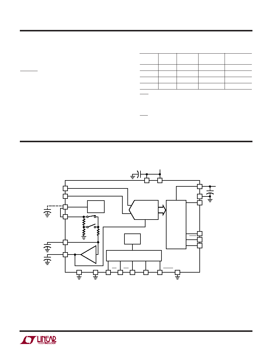
WU
U
TYPICAL CO
ECTIO DIAGRA
OTR
5V OR 3V
D13
OGND
OVDD
CONTROL LOGIC
2.5V
BANDGAP
REFERENCE
INTERNAL
CLOCK
14-BIT
ADC
OUTPUT
DRIVERS
REFOUT
14
+
–
PGA0
PGA1
CONVST
DGND
1411 TA01
AIN
+
AIN
–
AVP
DVP
5V
NAP
SLP
+
AVM
7, 8, 9
3
REFIN
22
F*
10
F
10
F
2k
5k
2
1
32
33
34
35
36
11
AGND
*A 22
F CAPACITOR IS NEEDED IF REFOUT IS USED TO DRIVE AIN–
31
26
BUSY
27
D0
25
12
28
29
4
REFCOM1
5
REFCOM2
6
+
30
10
+
X1.62/
X1.15
发布紧急采购,3分钟左右您将得到回复。
相关PDF资料
LTC1412IG#TR
IC ADC 12BIT 3MSPS SAMPLE 28SSOP
LTC1414IGN#TRPBF
IC A/D CONV 14BIT SAMPLNG 28SSOP
LTC1415CG#TRPBF
IC A/D CONV 12BIT SAMPLNG 28SSOP
LTC1416IG#TR
IC ADC 14BIT 400KSPS SMPL 28SSOP
LTC1417AIGN#TR
IC ADC 14BIT 400KSPS SMPL 16SSOP
LTC1418ACG#TRPBF
IC A/D CONV 14BIT SRL&PAR 28SSOP
LTC1419AISW#TRPBF
IC A/D CONV 14BIT SAMPLNG 28SOIC
LTC1420IGN#TRPBF
IC ADC 12BIT 10MSPS SAMPL 28SSOP
相关代理商/技术参数
LTC1412CG
功能描述:IC A/D CONV 12BIT SAMPLNG 28SSOP RoHS:否 类别:集成电路 (IC) >> 数据采集 - 模数转换器 系列:- 标准包装:1,000 系列:- 位数:12 采样率(每秒):300k 数据接口:并联 转换器数目:1 功率耗散(最大):75mW 电压电源:单电源 工作温度:0°C ~ 70°C 安装类型:表面贴装 封装/外壳:24-SOIC(0.295",7.50mm 宽) 供应商设备封装:24-SOIC 包装:带卷 (TR) 输入数目和类型:1 个单端,单极;1 个单端,双极
LTC1412CG#PBF
功能描述:IC A/D CONV 12BIT SAMPLNG 28SSOP RoHS:是 类别:集成电路 (IC) >> 数据采集 - 模数转换器 系列:- 标准包装:1 系列:microPOWER™ 位数:8 采样率(每秒):1M 数据接口:串行,SPI? 转换器数目:1 功率耗散(最大):- 电压电源:模拟和数字 工作温度:-40°C ~ 125°C 安装类型:表面贴装 封装/外壳:24-VFQFN 裸露焊盘 供应商设备封装:24-VQFN 裸露焊盘(4x4) 包装:Digi-Reel® 输入数目和类型:8 个单端,单极 产品目录页面:892 (CN2011-ZH PDF) 其它名称:296-25851-6
LTC1412CG#TR
功能描述:IC ADC 12BIT 3MSPS SAMPLE 28SSOP RoHS:否 类别:集成电路 (IC) >> 数据采集 - 模数转换器 系列:- 标准包装:1,000 系列:- 位数:12 采样率(每秒):300k 数据接口:并联 转换器数目:1 功率耗散(最大):75mW 电压电源:单电源 工作温度:0°C ~ 70°C 安装类型:表面贴装 封装/外壳:24-SOIC(0.295",7.50mm 宽) 供应商设备封装:24-SOIC 包装:带卷 (TR) 输入数目和类型:1 个单端,单极;1 个单端,双极
LTC1412CG#TRPBF
功能描述:IC A/D CONV 12BIT SAMPLNG 28SSOP RoHS:是 类别:集成电路 (IC) >> 数据采集 - 模数转换器 系列:- 标准包装:1,000 系列:- 位数:12 采样率(每秒):300k 数据接口:并联 转换器数目:1 功率耗散(最大):75mW 电压电源:单电源 工作温度:0°C ~ 70°C 安装类型:表面贴装 封装/外壳:24-SOIC(0.295",7.50mm 宽) 供应商设备封装:24-SOIC 包装:带卷 (TR) 输入数目和类型:1 个单端,单极;1 个单端,双极
LTC1412IG
功能描述:IC A/D CONV 12BIT SAMPLNG 28SSOP RoHS:否 类别:集成电路 (IC) >> 数据采集 - 模数转换器 系列:- 标准包装:1,000 系列:- 位数:12 采样率(每秒):300k 数据接口:并联 转换器数目:1 功率耗散(最大):75mW 电压电源:单电源 工作温度:0°C ~ 70°C 安装类型:表面贴装 封装/外壳:24-SOIC(0.295",7.50mm 宽) 供应商设备封装:24-SOIC 包装:带卷 (TR) 输入数目和类型:1 个单端,单极;1 个单端,双极
LTC1412IG#PBF
功能描述:IC A/D CONV 12BIT SAMPLNG 28SSOP RoHS:是 类别:集成电路 (IC) >> 数据采集 - 模数转换器 系列:- 标准包装:1,000 系列:- 位数:12 采样率(每秒):300k 数据接口:并联 转换器数目:1 功率耗散(最大):75mW 电压电源:单电源 工作温度:0°C ~ 70°C 安装类型:表面贴装 封装/外壳:24-SOIC(0.295",7.50mm 宽) 供应商设备封装:24-SOIC 包装:带卷 (TR) 输入数目和类型:1 个单端,单极;1 个单端,双极
LTC1412IG#TR
功能描述:IC ADC 12BIT 3MSPS SAMPLE 28SSOP RoHS:否 类别:集成电路 (IC) >> 数据采集 - 模数转换器 系列:- 标准包装:1,000 系列:- 位数:12 采样率(每秒):300k 数据接口:并联 转换器数目:1 功率耗散(最大):75mW 电压电源:单电源 工作温度:0°C ~ 70°C 安装类型:表面贴装 封装/外壳:24-SOIC(0.295",7.50mm 宽) 供应商设备封装:24-SOIC 包装:带卷 (TR) 输入数目和类型:1 个单端,单极;1 个单端,双极
LTC1412IG#TRPBF
功能描述:IC A/D CONV 12BIT SAMPLNG 28SSOP RoHS:是 类别:集成电路 (IC) >> 数据采集 - 模数转换器 系列:- 标准包装:1,000 系列:- 位数:12 采样率(每秒):300k 数据接口:并联 转换器数目:1 功率耗散(最大):75mW 电压电源:单电源 工作温度:0°C ~ 70°C 安装类型:表面贴装 封装/外壳:24-SOIC(0.295",7.50mm 宽) 供应商设备封装:24-SOIC 包装:带卷 (TR) 输入数目和类型:1 个单端,单极;1 个单端,双极